DSBSC demodulation by the
squaring means diode doubler technique
Here is yet another technique for the demodulation of
double sideband suppressed carrier signals . This is still the squaring
technique, where by a pair of diodes configured in a frequency doubling
configuration are used to generate the missing carrier that would appear
half way between the upper and lower sidebands .
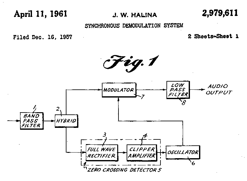
The technique i tried is based on patent No. 2979611
"Synchronous demodulation system ". issued to Joseph .W Halina by
the United States Patent office .
 .
.
My experiment involved a simple connection of components to achieve this .I
tested the circuit at 1.8 Mhz as my operational synchronous oscillator was
centered around 912 KHz from a previous experiment . The (2) Hybrid was a
simple 50 ohm resistive splitter , (7) the modulator or product
detector ,was an SBL-1 connected straight to an amplified
computer speaker system . The (3) full wave rectifier was the standard
twin, push push diode frequency doubler . I did not use a clipper
amplifier but relied on the good sensitivity of the (6) synchronous
oscillator, sub harmonically locking to the half frequency output of the
diode frequency doubler .
I constructed the diode frequency doubler using at
first a 1. 84 MHz centre tapped tuned circuit but for the life of me could
not get the output frequency after the diode summing, to be double the
input frequency . so I replaced the tuned circuit with a trifilar wound
transformer , and achieved the double frequency output . . I measured the input
power level and doubled output power level and obtained the conversion loss .
this is seen in the table underneath . Immediately I can see some sort of
active doubler amplification needs to be used to allow the use of radio
receiver Intermediate frequency 455 Khz power levels to enable good
reliable lock by the synchronous oscillator . It is a toss up as to just place a
20 dB IF amp stage before the diode doubler or incorporate the active
device in the doubling process as is in the Electronic design sept 1970 "simple
RF doubler" circuit by C Andren also in RSGB, Am ,Radio
Techniques Ed 5, pg 31 .
The diode doubler ,Input trifilar transformer was 24 turns of
fine twisted wire on a half inch core ( found in the junk box) the diodes
where BAT62 schottky diodes the output transformer was a bifilar
winding half inch , no real attempt at input/output matching was achieved
to optimise the doubler performance as I was just interested in testing basic
circuit principles .
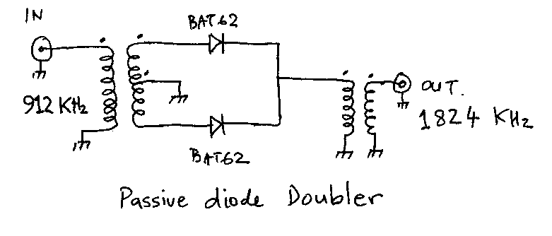
input 912 Khz
output 1824 Khz
isolation at 912Khz
+3 dBm
-13 dBm
-45 dB
0
-16.4
-43
-3
-19.2
-50
-6
-24
-53
-10
-31
-59
-13
-40
-67
-16
-52
-
-20
-71
-22
-78
-25
-84
-30
-96
The main reason I measured the isolation of the fundamental wrt to the output is
that I want the synchronous oscillator to lock onto the processed
frequency of 1824 KHz ( its subharmonic of 912 KHz ) and
not the bleed through of the fundamental 912 KHz ,
the 1824 KHz output is many db stronger in all cases so that
is not a problem .
The synchronous oscillator was built up using a BF494 Rf oscillator
transistor biased with a 100K resistor and a BC548 injection
transistor biased with a 10 Meg resistor . the BC548 has a much higher
Hfe than the BF494 so its biasing requirements are much less. I link
coupled off the synchronous osc tank coil with a couple of turns , this
produced a 3 dBm RF output level ,more than enough to operate the SBL-1
DBM.
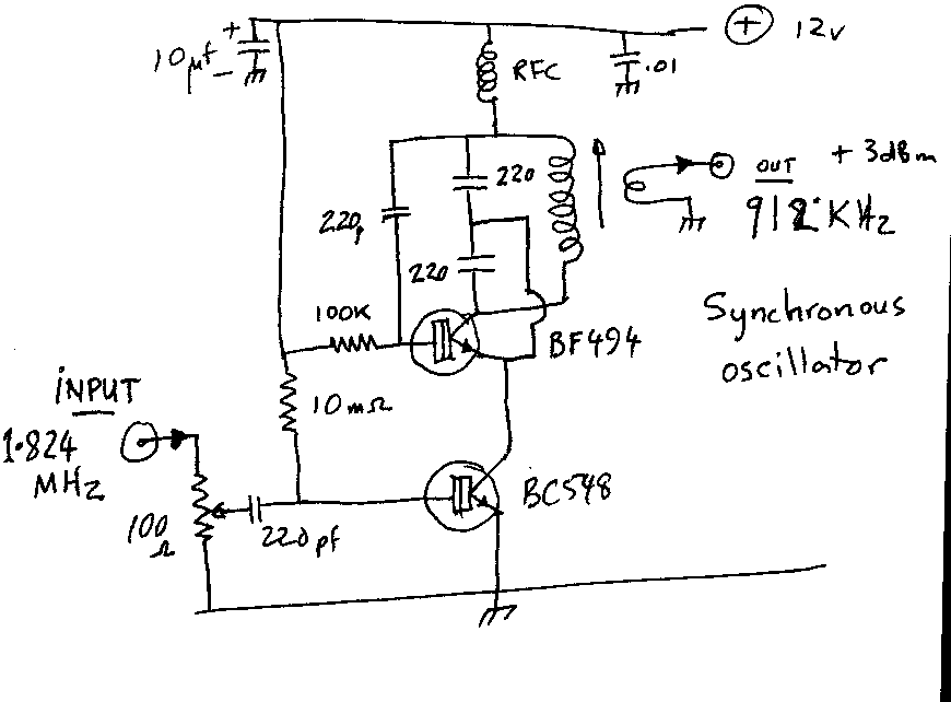
The synchronous oscillator
This oscillator can solidly lock to a -50 to
-40dbm signal and be pulled many KHz plus and minus before loosing
lock with the injection signal . the locked stability is such that the dsb
demodulated audio is clear and undistorted
I measured the fundamental suppression of the active
" Andren low cost full wave frequency doubler" as tried in my
other DSB demod circuit and found the suppression woefully inadequate using
unselected transistors( as would be expected ) I measured +3
dB !! no doubt this could be improved by placing a 1 k
ohm trimmer between the push- push emitters and the wiper to the collector
of the common current transistors , one may have to RF bypass the emitters
with capacitors ??? then maybe one could trim for maximum fundamental
suppression .
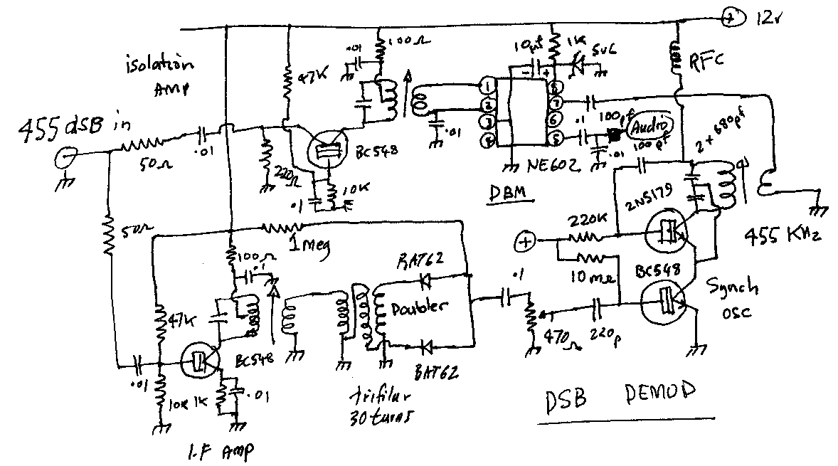
I will place a tuned IF amplifier stage ahead of the passive diode doubler
and thus make use of its excellent fundamental suppression and improve the
doubled " rf output" at the same time
I rebuilt the circuit below on double sided board to
investigate the concept
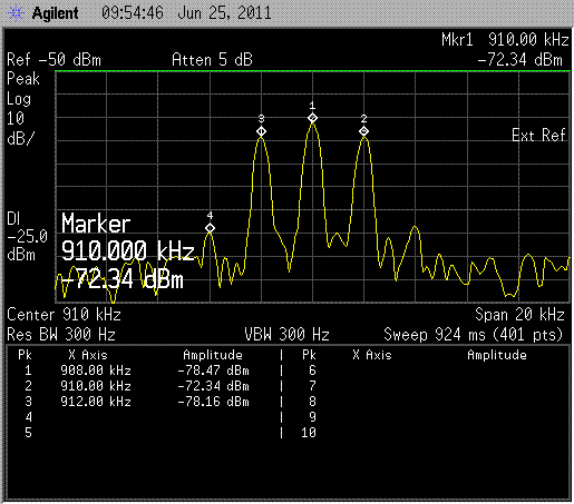
DSB input to circuit from HP8904A
at -28 dBm
spectrum output of diode frquency doubler
-42 dBm into board
The push push diode doubler enables the synthesis of the
wanted 10 Khz component of the summation of the upper and lower sidebands
, despite the input levels
the 910 Khz component is not strong and could be improve by narrow
filtering of the diode output and subsequent amplification . The doubler
set up is also susceptible to intermodulation though I didn't test to see if
this was a process of the pre doubler amplifier buckling under or
the diode doubler itself , either way if one overdrives the setup
..... wide band intermod appears at the output of the doubler
. see -28 dBm into board image
The synchronous oscillator has to look at this "junk" and decide which
sidband to lock to ! better to keep the input levels down (see the
-42 dBm image ) to make life somewhat easier
for the locking oscillator . i noticed when testing the demod board with
just the 1 Khz tone DSB the oscillator could be tuned to lock onto either
of the three signals visible on the -42 dBm into
board image .
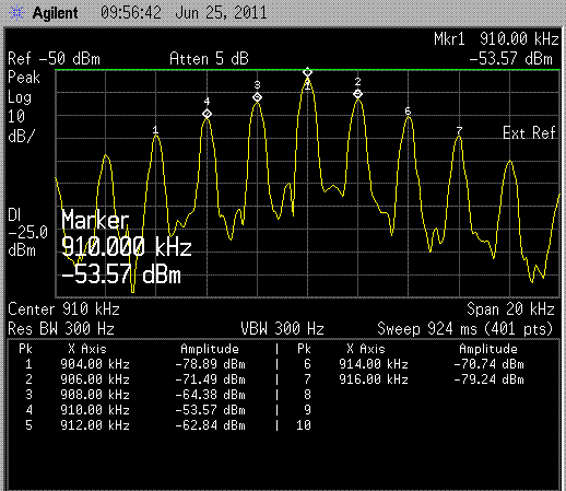
spectrum output of diode frquency
doubler -28 dBm into board
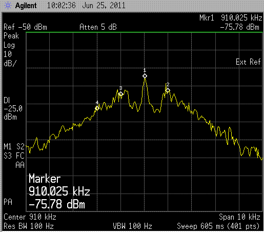
20 sec composite image comms audio at -42 dbm into board
note audio notches
I replaced the HP 8904a dsb source with a signal generator SRA-1 and
the audio coming out of my yeasu VX5 on the airband channel , i set
the spectrum analyser to max hold mode on the display and let the system run for
20 seconds , the comms audio built up the composite image above ,
note the audio notches either side of the synthesised carrier between 0
and 300 Hz ( actually 0 to 600 Hz because of doubling)
This circuit works very well i have yet to play with
the gains and losses of various parts of the circuit to make the principle
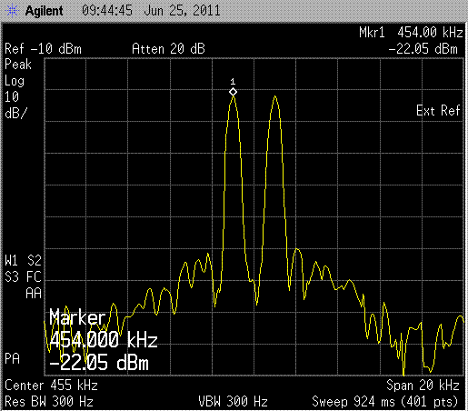
easily applied to the output of a 455 Khz transistor I.F. I
rebuilt up the complete circuit in double sided pc board at
455 and made the circuit above , The loss through the
doubler is quite drive dependant but I found by biasing the two schottky
diodes with a meg resistor from +12v improved the conversion by
almost 20dB at such low 455 Khz I.F levels . If I was going to
rebuild the circuit I would introduce some filtering at 910 Khz with one or two
ceramic filters and some post filter amplification before the synchronous
oscillator . to improve its locking range as the levels it has to work with in
the above circuit provide only a narrow lock range to compensate for drift ..
more to come
Double sideband demodulator mk3 squaring loop
Double Sideband suppressed carrier
demodulation , MC1496 as squaring means
back to home page

Double Sideband
suppressed carrier Demodulation Patents
These are all the References I can find on Double sideband
suppressed carrier demodulation , there are bound to be more , they are
all US patent Office registration No.. The E ones are European
Patent office ,
Have a look on the application of File dates and the Granting dates and some
people had to wait a long time before their patents were granted .
2924706 ,2992326, 2999155, 3047659, 3060383,
3088069, 3108158, 3141066, 3151217, 3252094, 3286183, 3345571, 3457513,
3537017, 3593149, 4253066
4821322, 4475218, 4642573, 4862098,
2979611,2397961, 4130839, 4430620, 4485487, 4510467, EP0291826B1, EP0293828B1,
2193801, 2276863, 2784311,
3375453 , 3430151,
3719903, a novel dsb modulator ,