NE567 AS AN EFFECTIVE RECEIVER MUTE
I have been experimenting with the NE567 as an FM demodulator off and on for a number of years already , The rebuild of our local Rotorua Br 33 , 2m linear
( multimode) Repeater has bought me to the requirement of design of an effective RF mute to enable the transmitter when a weak signal is received . In one of my write ups in my web pages you can see the use of the NE567 as an AM/FM demodulator and the demodulator performance figures as a simple 455Khz I.F . The NE567 has a lock function pin no. 8 which when receipt of a suitable signal of good S/N and over 26mV at the wanted frequency, will switch the internal transistor connected to pin 8 on, enabling the sink of current ie to drive a small relay or LED via a suitable dropping resistor . This could be used as an effective RF radio mute, but I find the mute opens and closes at a really good signal strength and as amateur operators, we want our radio mutes opening on relatively low signal to noise ratios .
The standard application of the NE567 wont allow this, how ever I have discovered a technique that would enable this
.I used to 10.7 MHz I.F output from the Branch 33 Linear
repeater receiver which I happen to have on my workbench at the
time.
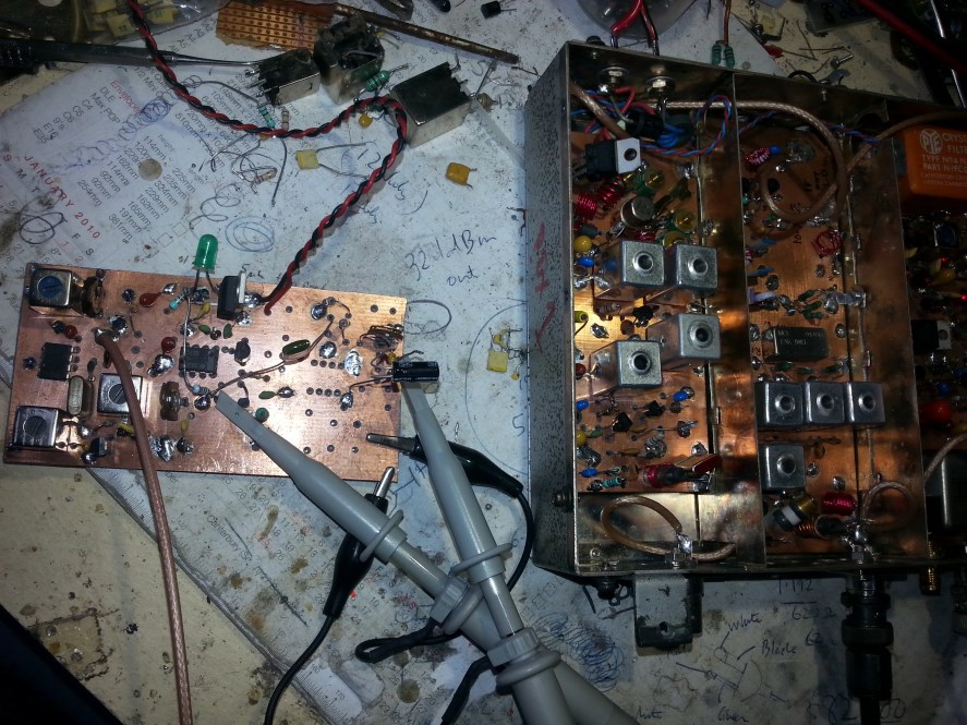
2m linear repeater receiver unit with 10.7 MHz out into NE567 demod board
10.7 MHz to 455Khz down converter
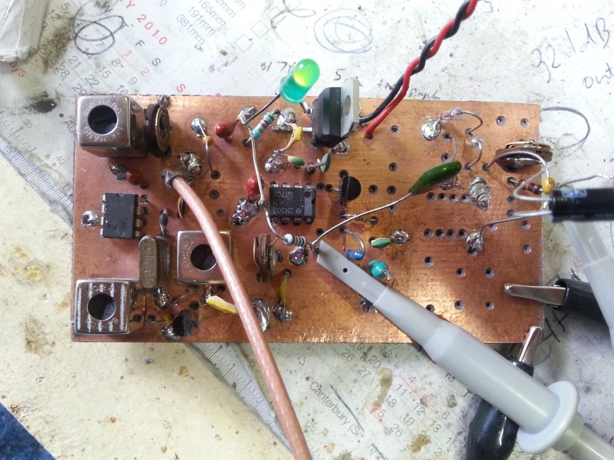
455 KHZ NE567 nbfm demod with
standard noise mute
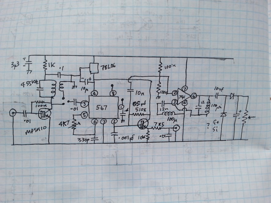
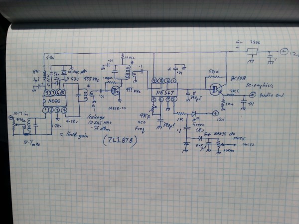
I built up an FM demodulator board with a NE612 mixer osc to shift the input frequency from 10.7 MHz to 455 KHz ,then into a single transistor MPSH-10 amp stage then into the NE567 PLL via a 455Khz I.F transformer. and connected the usual amplified high pass filter on the fm audio output, this of course feeds the usual diode doubler integrator that will switch a transistor opening the mute like a normal noise mute . Here is the circuit
above using an uA741 configured as high frequency noise band pass filter ,which gave me no end of trouble
To cut a long story short, I had a green led connected to the lock pin no.8 so when I adjusted VCO frequency or RF input level , I had an extra visual indication of the operation of the pll . I also monitored for demodulated audio at 2.5KHz deviation and the quieting . when a signal is tuned , rf amplitude varied .and VCO tuned .Via
the NE612 down conversion stage ahead of the NE567 I noticed
there is an interaction of the 10.7 MHz rf level input and the centre frequency of the 455 KHz VCO. .Variables can be tweaked to optimise results.
At the same time I had two channels of the oscilloscope monitoring various parameters . demodulated output, high pass Amp noise output etc . There was good quieting of the carrier at low signal levels (-122 dBm)and that should be suitable as a mute function ,but its use eluded me. After many hours of fiddling to say the least , and not achieving a RELIABLE result wrt to the detection of weak signals, frustration caused me to started looking at the lock light as some sort of alternative. So I put the probe onto the LED ( pin8 ) and I played around with rf levels .What I noticed on the
oscilloscope is a series of voltage spikes whose quantity varied in proportion to the amount of RF input,. As the signal gets stronger the spikes become less in number and the transistor starts to stay turned on more and more as the signal increases, to a situation where the pin 8 is completely switched on and the LED reaches full brilliance ..usually at 26 mV input as the data sheet says.
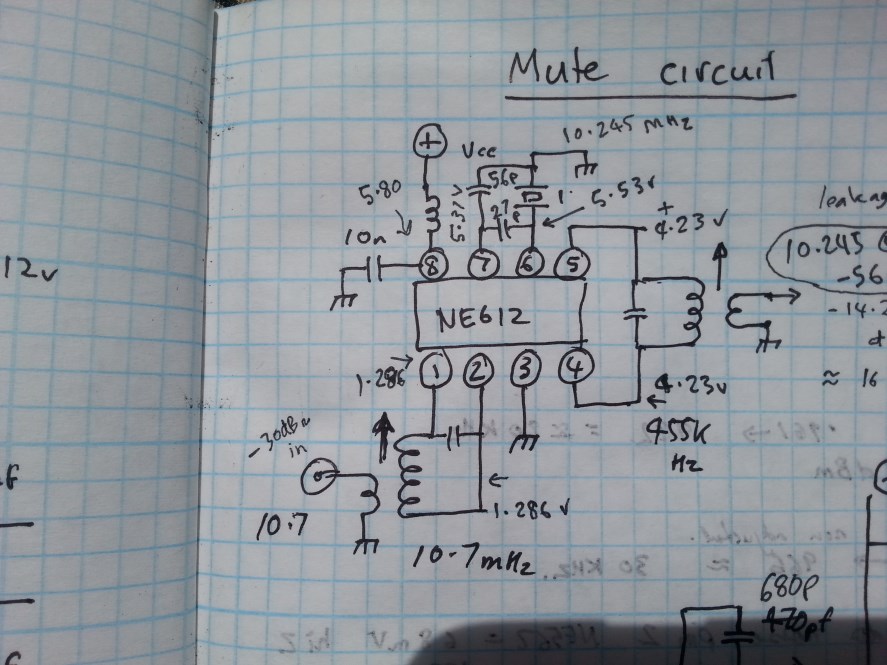
NE612 down converter to 455 Khz
But at this level the S/N is much to high to be of use and we need the mute to open when the signal is weaker. Enter the integrator on the output of pin 8 !! The 741 and all its associated high pass frequency circuitry was removed and the output of the pin 8 at where the resistor connects to the led, was connected by a .01 cap to the integration diode input . Thus the pulse width modulation of the pin8 lock integration was converted to a D.C output and monitored by the ‘scope. Below is the integration output at
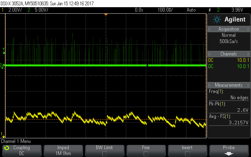
No signal input, to the 2m linear repeater receiver I took my signal
output from the I.F output BNC,. I noticed that if you over drive the input to the NE567 you can saturate the AM detector that drives pin 8 and you will not get any variation on spikes with the manual change in VCO frequency around the lock frequency of 455 Khz, so back of the RF level so you see the lock light brightness begin to dim.
No Signal into the demodulator
.
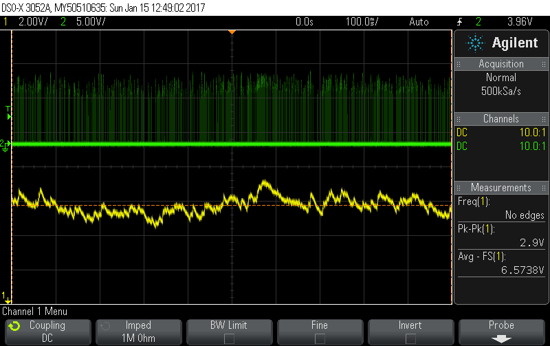
Channel one (yellow) is set to 2v per division and from no signal to –126 dBm at 144.950 MHz it has changed by 4 volts !!
then fed a signal of –126 dBm from the Agilent N9310A signal
generator into the 2m receiver and this is what I saw as the result .The green
trace is the output of pin 8 looking at the output spikes a very respectable change and most useable
.Note the change in the density of spikes from the NE567 AM synchronous detector
!! this is coming out of the 1.Q detector !!!!
!! The Agilent N9310A has some very good features such as sweep mode , this can be set as individual steps of a to and from range or individual “frequencies” so I set it as just two two steps 144.350 Mhz and 144.950 Mhz and set the dwell to 0.5 second on each frequency ,Thus the 2m linear repeater receiver will receive a frequency and then no frequency . A signal at –126 dbm and no signal . The demod board has a variable rf input pot of 470 ohm and the VCO has a 4k7 adjustment pot , I have adjusted the voltage level and the VCO frequency to achieve the best result , The input to the demod board is from an AGC control receiver . with an I.F output of –40 dBm at 10.7 MHz with no signal.
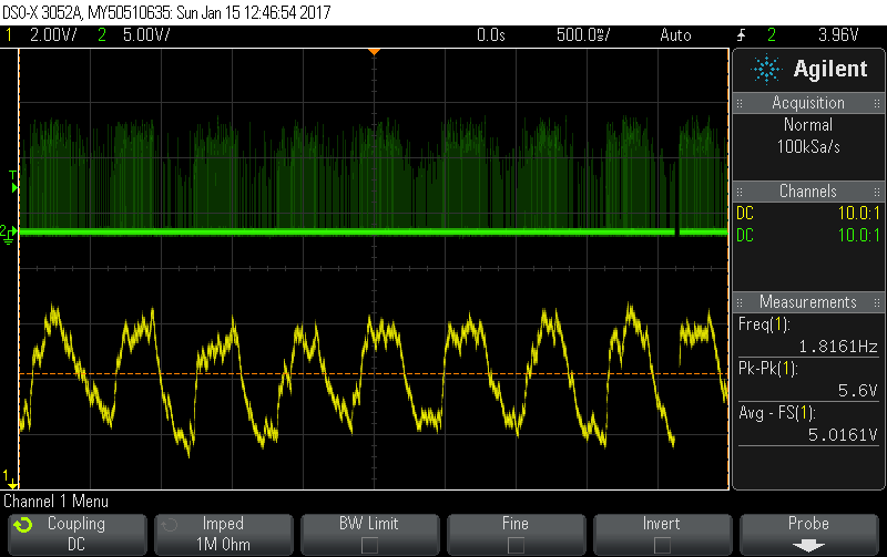
This is the on –off output of the demod board with an input of –126dbm on and then no signal alternately.
What you can now see is a very respectable response of the NE567 to weak RF input signals with low carrier to noise ratio.
this is exactly what we want for our receiver project and you can also see how simple the resulting circuitry actually is !!
There is a filter capacitor on pin 2 ,it is responsible for the loop bandwidth ,on my board I have used 390 Pf changed from 1nF ,though this value could be optimised for performance , There is also a capacitor on pin1 which is an integration capacitor for the output of the internal AM synchronous demodulator .on my circuit this was 10nf I have not optimised the value ,so variation could improve performance ??
All I have to do is now place some simple switching circuitry after the diode integrator variable resistor and the required function at low signal level is achieved .
final version of low level mute using NE567
I suspect it could be advantageous using an RF limiter
or AGC system ahead of the NE567 you could have a simple pot to
adjust the maximum signal into the NE567 under full limiting so you
didnt overdrive the synchronouus demod mixer and thus get a good
range of squelch adjustment
back to home page